Abstract 1. Lattice strain control catalyst activity (Directandcontinuousstraincontrolofcatalystswithtunablebatteryelectrodema...
1. Lattice strain control catalyst activity
(Direct and continuous strain control of catalysts with tunable battery electrode materials)
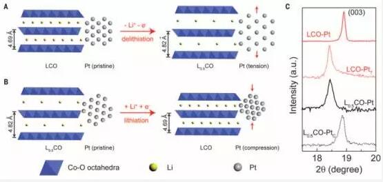
Professor Cui Wei of Stanford University recently reported that the cell strain (LiCoO2) is used to directly and continuously control the lattice strain of the Pt catalyst, thereby regulating the catalytic activity of Pt for the oxygen reduction reaction (ORR). The conventional method of using a metal coating layer causes strain and causes a ligand effect, and the volume change caused by the electrochemical conversion method of the charged discharge electrode material can be precisely controlled to regulate the catalyst supported on the electrode material. Compressive strain or tensile strain. LiCoO2 has about 5% lattice compression and tensile strain during charge and discharge, which causes the lattice of Pt nanoparticles to also undergo corresponding strain. They observed this change using spherical aberration-corrected transmission electron microscopy, and electrochemical tests showed that Pt has a 90% improvement in catalytic performance for oxygen reduction under compressive strain and a 40% reduction in catalytic performance under tensile strain. . These results are also consistent with theoretical calculations. (Science DOI: 10.1126/science.aaf7680)
2. Current induced inversion in magnetic insulators
(Current-induced switching in a magnetic insulator)

The spin Hall effect in heavy metals converts the charging current into a pure spin current and then injects it into an adjacent ferromagnet to apply torque. This spin-orbit torque (SOT) has been widely used to manipulate magnetization in metal ferromagnets. In the case of a magnetic insulator (MI), although the charging current cannot flow, the spin current can be transmitted, but the magnetization in the current induced control MI has not been achieved so far. Can Onur Avci et al. demonstrated that a charging current in a platinum blanket drives a spin current generated in a vertically magnetized yttrium iron garnet film to induce conversion. Estimating using spin Hall magnetoresistance and harmonic Hall measurements, the film has relatively large spin-mixed conductance and damped SOT, indicating significant spin transparency at the Pt/MI interface. They also show that at low current densities, the spin current injected through this interface leads to deterministic magnetization reversal, laying the foundation for MI-based ultra-low dissipation spintronic devices. (Nature Materials DOI: 10.1038/NMAT4812)
3. Doped polymer semiconductor with ultra-high and ultra-low work function ohmic contact
(Doped polymer semiconductors with ultrahigh and ultralow work functions for ohmic contacts)
In order to manufacture a high performance semiconductor device, a good ohmic contact between the electrode and the semiconductor layer is required to introduce a maximum current density through contact. Achieving ohmic contacts requires injecting holes and electrons from electrodes having high and low work functions, respectively, where the work function is the minimum energy required to move electrons from the Fermi level of the electrode to the vacuum level. However, it is very challenging to fabricate a conductive film having a sufficiently high or low work function, particularly for solution processing semiconductor devices. Hole-doped polymer organic semiconductors are available in a limited range of work functions, but hole-doped materials with ultra-high work functions, especially electron-doped materials with ultra-low work functions, are not yet available. A key challenge is to control dedoping and inhibit dopant migration to stabilize the film. Tang et al. proposed a simple method to overcome these limitations to achieve a wide range of work function doping films in the range of 3.0-5.8 electron volts by doping the conjugated polyelectrolyte. Internal ion exchange then produces a self-compensating heavily doped polymer. The mobile carriers on the polymer backbone in these materials are compensated by covalently bonded counterions. Although their proposed self-compensating doped polymer surface is similar to a self-doping polymer, this polymer is produced by separate charge carrier doping and compensation steps, enabling the use of strong dopants. A very high or very low work function is achieved. The work of Cindy G. Tang et al. provides a means of producing ohmic contacts that can be used not only for organic semiconductors, but also for other advanced semiconductors, including perovskites, quantum dots, nanotubes, and two-dimensional materials. (Nature DOI: 10.1038/nature20133)
4. High efficiency and high stability of CsSnI3 perovskite solar cells
(Enhanced stability and efficiency in hole-transport-layer-free CsSnI3 perovskite photovoltaics)

Although a large amount of research work has increased the power conversion efficiency of lead perovskite photovoltaic power generation to more than 20%, photovoltaic technology based on tin halide perovskite has not yet benefited from such in-depth research results. This is mainly due to the sensitivity of the tin halide perovskite to oxidation, the low energy of defect formation, and the difficulty in forming a pinhole-free film. In view of this, Marshall et al. demonstrated a CsSnI3 perovskite photovoltaic device with no hole selective interfacial layer. This device exhibits approximately 10 times more stability than devices using the same structure of methylammonium iodide lead perovskite and exhibits the highest photovoltaic efficiency of the CsSnI3 device to date: 3.56%. The latter is mainly due to the high device fill factor, which is an additional treatment that minimizes the pinhole density in the perovskite film by using an electron blocking layer or based on co-deposition of the perovskite precursor with SnCl2. The steps are implemented. These two findings raise the prospects for practical use of this type of lead-free perovskite photovoltaic. (Nature Energy DOI: 10.1038/NENERGY.2016.178)
5. Entropy contribution enhances the polarity compensation of CeO2(100) plane
(Entropic contributions enhance polarity compensation for CeO2(100) surfaces)
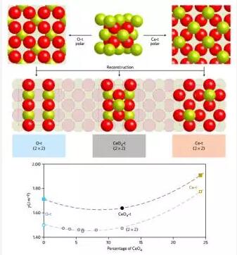
The surface structure of the material controls the physical and chemical response of the material. Surface polarity terminals are attractive because of their distinctive properties, but they are inherently unstable. Metallurgy, adsorption and ordered reconstruction can eliminate the negative effects of thermodynamics and stabilize the polar surface. For CeO2(100), Marçal Capdevila-Cortada et al. proposed a complementary stabilization mechanism based on surface disorder, which has been theoretically simulated: explaining surface energy and configuration entropy, demonstrating the importance of ion distribution degeneracy, A low diffusion barrier between the structures that ensure equilibrium is identified. The disordered structure in the oxide can also be further stabilized by preferentially adsorbing water. For surfaces with a large number of vacancies, an entropy stabilization term will appear. Assessing the effects of surface disturbances remains a challenge when establishing new structure-activity relationships. (Nature Materials DOI: 10.1038/NMAT4804)
6. High-resolution three-dimensional structure microscope
(High-resolution three-dimensional structural microscopy by single-angle Bragg ptychography)
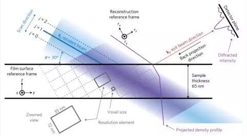
Coherent X-ray microscopy with phase recovery of Bragg diffraction intensity enables three-dimensional imaging of lattice distortion within the crystal at nanoscale spatial resolution. While this capability can be used to address nanoscale structure-property relationships, rigorous data measurement requirements may limit the application of existing methods. Hruszkewycz et al. introduced a three-dimensional (3D) Bragg projection overlay imaging (3DBPP) method for efficient 3D imaging of nanoscale lattice properties and strain fields in crystalline materials. The method enables 3D image reconstruction of the crystal volume from a series of two-dimensional X-ray Bragg coherence intensity diffraction patterns measured at a single incident beam angle. The structural information of the sample is encoded by the scanning beam along two reciprocal spatial directions perpendicular to the Bragg diffraction exit beam and along a third dimension in real space. At the same time, Hruszkewycz et al. also provided analytical derivation, numerical demonstration and experimental reconstruction of lattice distortion in nanoelectronic prototype equipment components for their proposed methods. (Nature Materials DOI: 10.1038/NMAT4798)
7. Reduce the efficiency of organic photovoltaic cells - stability - cost gap
(Reducing the efficiency–stability–cost gap of organic photovoltaics with highly efficient and stable small molecule acceptor ternary solar cells)

If you want to deploy the technology of organic photovoltaic modules, you need to improve the light conversion efficiency and stability of the device, while keeping the cost of the material low. Baran et al. demonstrated a ternary method for achieving high efficiency and high stability of solar energy points, where the ternary includes two non-fullerene acceptors, and a scalable and ligandable donor polymer, ie poly( 3-hexylthiophene) (P3HT), as well as high efficiency low band gap polymers, are included in monolayer heterojunction devices. The addition of an absorbing small molecule acceptor to the P3HT-based non-fullerene blend resulted in an increase in device efficiency of 7.7 ± 0.1% without any solvent additives. Such improvements are attributed to changes in microstructure, including reduced charge recombination and increased photovoltage, as well as improved light collection throughout the visible region. The stability of P3HT-based devices under ambient conditions is also significantly improved relative to polymer: fullerene devices. The two mixed acceptors are combined with a low band gap donor polymer (PBDTTT-EFT, also known as PCE10) such that the solar cell has an efficiency of 11.0 ± 0.4% and a high open circuit voltage of 1.03 ± 0.01V. (Nature Materials DOI: 10.1038/NMAT4797)
Detection of electron and catalytic properties of bimetallic surfaces at 8.3 nm resolution
(Probing the electronic and catalytic properties of a bimetallic surface with 3 nm resolution)
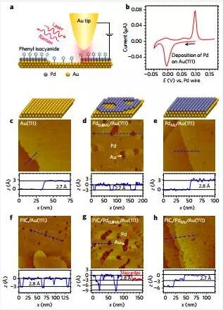
Understanding heterogeneous catalysis at the atomic and molecular scale is necessary to characterize the active sites and improve catalyst design. Achieving such precise scales requires specific techniques to correlate catalytic performance with specific surface structures to avoid averaging effects. Tip-enhanced Raman spectroscopy (TERS) combined with a plasma-enhanced Raman scattering scanning probe microscope provides both topographic and chemical information in a variety of environments at the nano/atomic scale. This technique has been used to monitor catalytic reactions and to establish the relationship between local structures and heterogeneous catalyst functions. Bimetallic catalysts, such as Pd-Au, exhibit excellent catalytic performance in various catalytic reactions. However, due to the complexity of the structure, it is still very challenging to construct the relationship between structure and reactivity. The Ren research team at Xiamen University used TERS technology to detect the chemical and physical properties of specific active sites under atomic resolution. They used isonitrileized benzene as a probe molecule to detect the physicochemical properties of Pd/Au bimetallic catalysts at 3 nm resolution. They observed an increase in the reactivity of a weakened N≡C bond and isocyanated benzene at the Pd ladder boundary. Density functional theory reveals that the lower coordination step boundary Pd atoms have higher d-band electron structures, confirming these observations. (Nature Nanotechnology DOI: 10.1038/NNANO.2016.241)
This article is authorized by the new material online (micro signal: xincailiaozaixian), if other media need to reprint, please contact the new material online small series (micro signal) Short-wave Pass Linear Gradient Filter
The short-wave pass linear gradient filters are continuously coated to achieve spatially continuous variation of filtering characteristics based on a multi-layer wedge-shaped film structure. The slope of the film can be adjusted according to the dispersion requirement to obtain the target linear rate of change. The Linear Gradient Filter is highly integrated and has an irreplaceable advantage in the miniaturization and lightweight design of spectroscopy instruments. The products are widely used in lightweight hyperspectral imaging spectrometers, portable spectrometers, and medical endoscopes.
Short-Wave Pass Linear Gradient Filter,Short Pass Optical Filter,Bandpass Filter Kit,Gradient Filters
Changchun Champion Optics Co.,Ltd , https://www.champion-optics.com