Daily discussion of photovoltaic power generation, do you know the principle of solar cell power generation? This article introduces the power generation principle of crystalline silicon solar cells in text format. It belongs to science level and is very easy to understand.
Solar cell power generation principle
First, N-type semiconductors and P-type semiconductors
Purely pure semiconductors with a crystal structure, called intrinsic semiconductors, form covalent bonds between atoms. Their structures are shown in Figure 1-3. Two electrons in a covalent bond are called valence electrons.
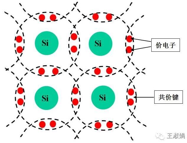
Figure 1: Intrinsic semiconductor structure
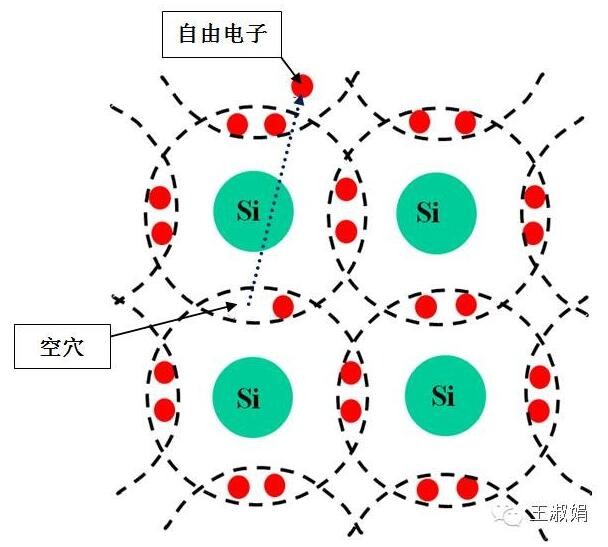
When valence electrons get certain energy (temperature rise or light exposure), they can break free from the binding of nuclei, become free electrons (negative charge), and at the same time leave a vacancy in the covalent bond, which is called hole (positive charge). , as shown in Figure 1-4. Both free electrons and holes are called carriers. The number of carriers in intrinsic semiconductors is very small, and their electrical conductivity is poor. Figure 2: Free electrons and holes formed after valence electrons are excited
The intrinsic semiconductor is doped with a trace amount of impurities (elements) to form an impurity semiconductor, which can greatly enhance its electrical conductivity.
Incorporating pentavalent phosphorus in place of the silicon atom, four of the five outer electrons in the outer layer of the phosphorous atom form covalent bonds with the surrounding semiconductor atoms, and one more electron is almost unconstrained and can easily become a free electron. . Therefore, the number of free electrons after doping is greatly increased, and free electron conduction becomes the main conductive method of this semiconductor, which is called an N-type semiconductor.
When trivalent boron is incorporated in place of the silicon atom, the three outer electrons of the outer layer of the boron atom form covalent bonds with the surrounding semiconductor atoms, creating a "hole." Therefore, after the doping, the number of holes is greatly increased, and the hole conduction becomes the main conduction mode of this semiconductor, which is called a P-type semiconductor.
Regardless of whether the N-type or P-type semiconductors are neutral, they do not display electricity.
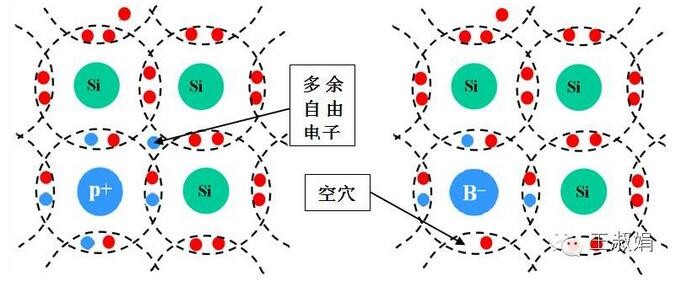
Figure 3-1a: N-type semiconductor Figure 3-2b: P-type semiconductor
N-type semiconductor electrons are many sons, holes are the minority;
P-type semiconductors have many holes and electrons are few.
Second, "PN junction" and "photovoltaic effect"
The PN junction is composed of an N-type doped region and a P-type doped region in close contact. On a complete silicon wafer, an N-type semiconductor is formed on one side and a P-type semiconductor is formed on the other side with different doping processes. The region near the interface between the two semiconductors is a PN junction. The basic structure of a solar cell is a large planar PN junction.
When sunlight hits the PN junction, the PN junction absorbs light energy to excite electrons and holes, creating a voltage in the PN junction called the "photovoltaic effect" or simply the "photovoltaic effect."

Figure 4: Principle of Photovoltaic Power Generation
Linear light is a type of Pendant Light that is primarily made of lines and is usually made of materials such as metal, wood, or plastic. The design of the linear light is simple and modern, suitable for various interior decoration styles, especially for modern minimalist style homes. The shape of the linear light is diverse, it can be straight, curved, or a combination of multiple lines to form a complex shape. The light of the linear light is soft and uniform, suitable for lighting in places such as living rooms, dining rooms, and study rooms.
Linear Pendant Light,Flush Linear Light Fixture,Linear Light Fixture For Dining Room,Linear Light Ceiling
Zhengdong Lighting Co., Ltd. , https://www.sundint.com